
Several technical or production-related demands require the covering / sealing of vias. These types of Via covering are possible:
- Via Tenting (simple covering)
- Via Plugging (partially filled)
- Via Filling (completely filled)
In the following, you will find a comparsion of the technical capabilities.
The reference is the IPC 4761, which can be purchased here: https://portal.ipc.org/Association/Index.htm.
Abstract
| Type | Description | Covering-Material |
|---|---|---|
| I-a / -b | Tented one-sided / double-sided | Dryfilm solder-stop |
| II-a / -b | Tented & Covered one-sided / double-sided | Dryfilm solder-stop + LPI solder-stop |
| III-a / -b | Plugged one-sided / double-sided | Plugging Epoxy (non-conducting paste) |
| IV-a / -b | Plugged & Covered one-sided / double-sided | Plugging Epoxy + LPI solder-stop |
| V | Filled | Plugging Epoxy (non-conducting paste) |
| VI-a / -b | Filled & Covered one-sided / double-sided | Plugging Epoxy + LPI solder-stop |
| VII | Filled & Capped | Special Plugging Epoxy + plating |
Via Covering Types

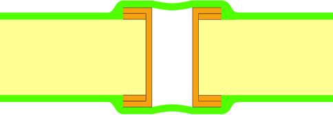
IPC 4761 Type I: Tented Via
The via is completely covered with dryfilm solder-stop.
One-sided: Type I-a
Double-sided:Typ I-b

IPC 4761 Type II: Tented & Covered Via
The via is completely covered with dryfilm solder-stop and overprinted with normal solder-stop, afterwards.
One-sided: Type II-a
Double-sided:Type II-b
Application
- Protection of solder floating up to the component side
- Enables vacuum-adaption for production
- Covering of critical vias, e.g. beneath BGA
Alternatives
You can apply Via Filling, alternatively.
Through cutting the solder-stop clearance, you can ensure a sufficient solder-stop bridge for BGAs. Using this method, the via annular rings will be partly covered with solder-stop.
Parameters
| Covering | Max. Drill-Ø |
|---|---|
| Via Tenting | 300µm |
Designation
It is sufficient to cover the vias within the solder-stop layer.


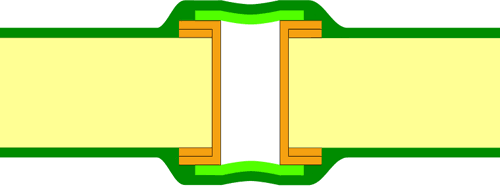
IPC 4761 Type III: Plugged Via
The via is partially filled with non-conductive paste.
One-sided: Type III-a
Double-sided: Type III-b

IPC 4761 Type IV: Plugged & Covered Via
The via is partially filled with non-conductive paste and overprinted with normal solder-stop, afterwards.
One-sided: Type IV-a
Double-sided: Type IV-b
Multi-CB recommends one-sided plugging (Type III-a / Type IV-a) as there is a chance of cracks through encapsulated gas while soldering double-sided plugged vias.
Application
- Protection of solder floating up to the component side
- Enables vacuum-adaption for production
Parameters
| Covering | Min. Drill-Ø | Max. Drill-Ø |
|---|---|---|
| Via Filling | 250µm | 500µm |
Designation
Copy the vias to be filled into an additional layer and define that layer with your order.

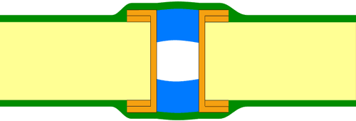
IPC 4761 Type V: Filled Via
The via is filled completely with non-conductive paste.


IPC 4761 Type VI: Filled & Covered Via
The via is filled completely with non-conductive paste and overprinted with normal solder-stop, afterwards.
One-sided: Type VI-a
Double-sided: Type VI-b

IPC 4761 Type VII: Filled & Capped Via
The via is plated-through and cleaned - afterwards a non-conductive paste is forced in and hardened - the ends are planarized, metallized and plated-over. Hence, the surface is planar and solderable.
This technology is mostly used for Via-in-Pad solutions and is also applied for stacked und staggered (Micro-)vias. Via Plugging faciliates routing of additional conductor traces between BGA vias amongst other things.
Filled & Capped Vias are also possible for Blind Vias.


Parameters
| Covering | Min. Drill-Ø | >> Pad-Ø | Max. Drill-Ø | >> Pad-Ø | Aspect ratio | |
|---|---|---|---|---|---|---|
| Filled & Capped IPC 4761 Type VII | 150µm | 350µm | 400µm | 600µm | 1:12 | |
| Filled & Capped electroplated | 100µm | 300µm | - | - | 1:10 |
Designation
Copy the vias to be plugged into an additional layer and define that layer with your order.