
BGAs (Ball Grid Arrays) are SMD components with connections on the bottom of the component. Each pin is provided with a solder ball. All connections are distributed in a uniform surface grid or matrix on the component. Common grids are nowadays: 1.27 mm - 1.00 mm - 0.80 mm - 0.50 mm.
With several hundred component connections, the number of „routable" pins is limited per layer. The inner pins of the BGA can only be connected through a via and routed to another layer > DogBone technology.
If the pitch is even smaller, or if traces between the solder pads are necessary, the via-in-pad technology is recommended: The vias are placed directly into the solder pads of the BGA.
Manufacturer's instructions must be followed carefully. These define the elementary connection distances, solder ball diameters and the housing geometries. Other technical details such as technology of the vias or trace -width and -spacing will be specified by the designer. For possible parameters check the following tables.
BGA: Design proposal
The values given are design proposals, values of component data sheets are always preferable.
| Pitch | Ø BGA-Pad* | Ø Via-Pad / Via-Drill | Ø Via-Pad**/ Via-Drill | Track-width / -space | Track-width / -space |
|---|---|---|---|---|---|
 | Dog-Bone | Via-in-Pad |  |  | |
| 1.27mm | 550µm | 550µm/300µm | - | 150µm/285µm | 150µm/140µm |
| 1.00mm | 500µm | 500µm/200µm | - | 150µm/175µm | 100µm/100µm |
| 0.80mm | 350µm | 450µm/150µm | 400µm/200µm | 150µm/100µm | 70µm/70µm |
| 0.50mm | 250µm | 250µm/100µm | 300µm/100µm | 70µm/90µm | - |
| 0.40mm | see below | see below | see below | see below | see below |
*plus 50µm circumferential solder-stop clearance
**plus 50µm circumferential solder-stop clearance, please order as IPC 4761 Type VII: Filled & Capped Vias
BGA Dogbone - Detail
Outer layers

| Pitch = | 1.27mm | 1.00mm | 0.80mm | 0.50mm | |
|---|---|---|---|---|---|
| a | Ø BGA Pad (solder pad) | 550µm | 500µm | 350µm | 250µm |
| b | Solder-stop (SS) clearance, circumferential | 75µm | 75µm | 75µm | 75µm |
| c | Ø Solder-stop clearance | 700µm | 650µm | 500µm | 400µm |
| d | Stringer length (approx.) | 348µm | 207µm | 165µm | 103µm |
| e | Ø Via Pad | 550µm | 500µm | 450µm | 250µm |
| f | Ø Via Pad drill (final) | 300µm | 200µm | 150µm | 100µm |
| g | Via Pad <> BGA Pad | 348µm | 207µm | 165µm | 103µm |
| h | Stringer width | 250µm | 250µm | 200µm | 150µm |
| i | SS clearance <> SS clearance | 570µm | 350µm | 300µm | 100µm |
| j | Via Pad <> Via Pad | 720µm | 500µm | 350µm | 250µm |

Inner layers
Fan-Out with 1 track
| Pitch = | 1.27mm | 1.00mm | 0.80mm | 0.50mm | |
|---|---|---|---|---|---|
| e | Ø Via Pad | 670µm | 550µm | 425µm | 260µm |
| b | Ø Via Pad Drill | 300µm | 250µm | 150µm | 100µm |
| k | Track Width | 200µm | 150µm | 125µm | 80µm |
| l | Track Space | 200µm | 150µm | 125µm | 80µm |

Inner layers
Fan-Out with 2 tracks
| Pitch = | 1.27mm | 1.00mm | 0.80mm | 0.50mm | |
|---|---|---|---|---|---|
| e | Ø Via Pad | 620µm | 485µm | 300µm | - |
| b | Ø Via Pad Drill | 300µm | 250µm | 150µm | - |
| k | Track Width | 125µm | 100µm | 100µm | - |
| l | Track Space | 125µm | 100µm | 100µm | - |

Inner layers
Fan-Out with 3 tracks
| Pitch = | 1.27mm | 1.00mm | 0.80mm | 0.50mm | |
|---|---|---|---|---|---|
| e | Ø Via Pad | 550µm | 460µm | 275µm | - |
| b | Ø Via Pad Drill | 250µm | 200µm | 100µm | - |
| k | Track Width | 100µm | 75µm | 75µm | - |
| l | Track Space | 100µm | 75µm | 75µm | - |
BGA 0.4mm Pitch
The PCB design for BGA with 0.4mm pitch is special production and requires the use of HDI-Technology and Via-in-Pad. Please always consult our technical department.
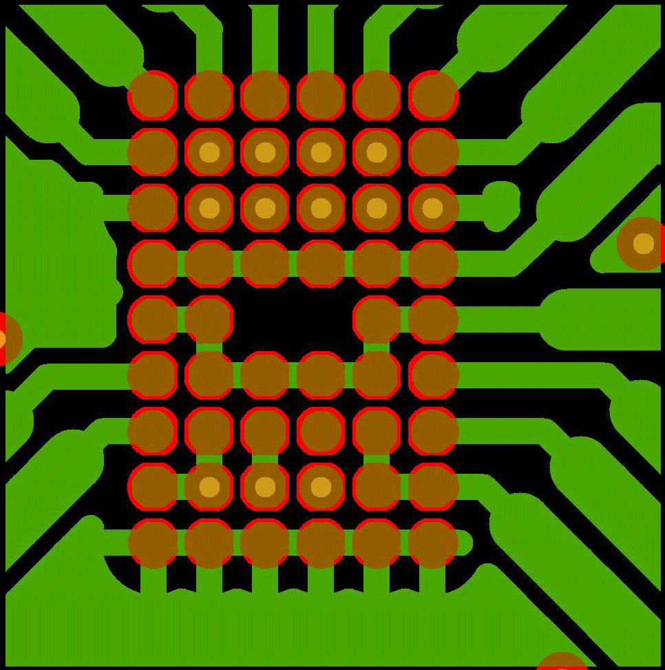
BGA 0.4mm Pitch - Production example
TOP-Side of PCB
- BGA with 0.4mm Pitch
- Via-in-Pad (Filled & Capped Vias)
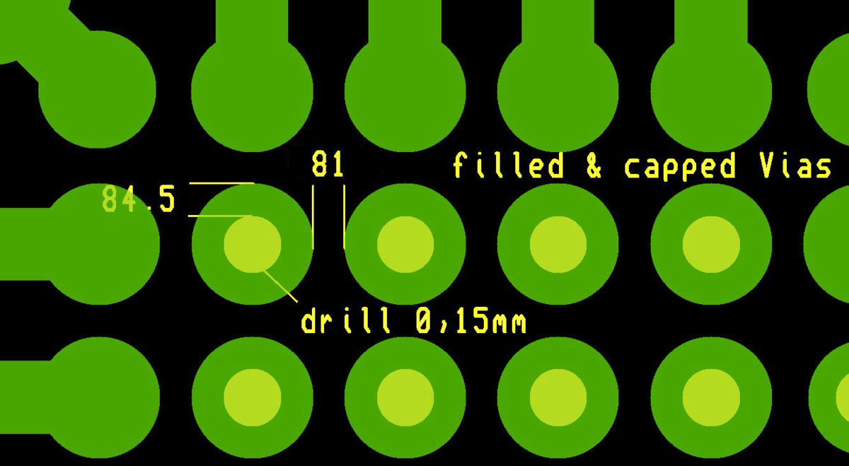
TOP-Side Detail
- Drill: 0.15mm
- Annular ring: 84.5µm
- Via-Pad: 319µm
- Copper to copper: 81µm
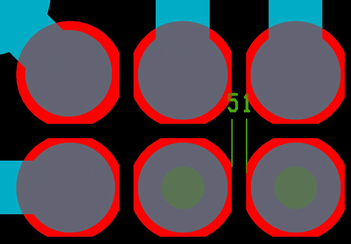
TOP-Side solder-stop
- Solder-stop bridge: 51µm
- Solder-stop clearance: 19µm
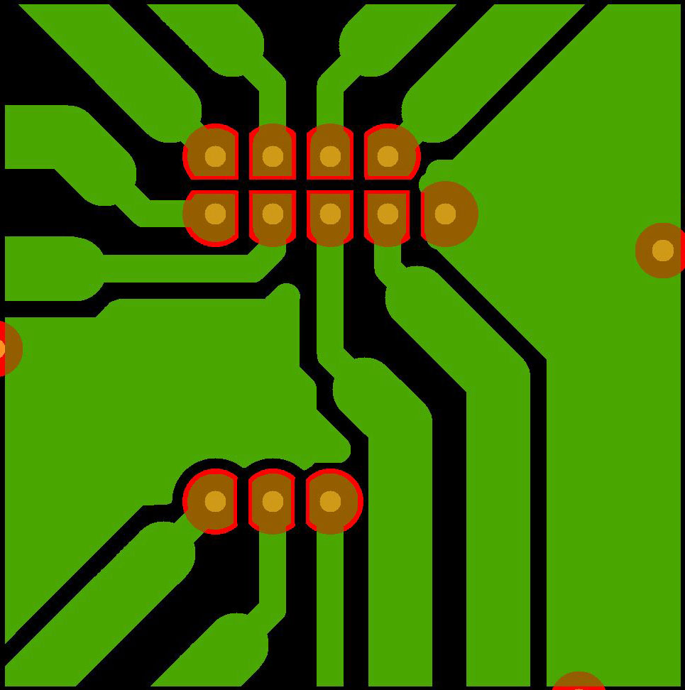
BOT-Side of PCB
Routing of 0.4mm pitch BGA with maximum parameters.
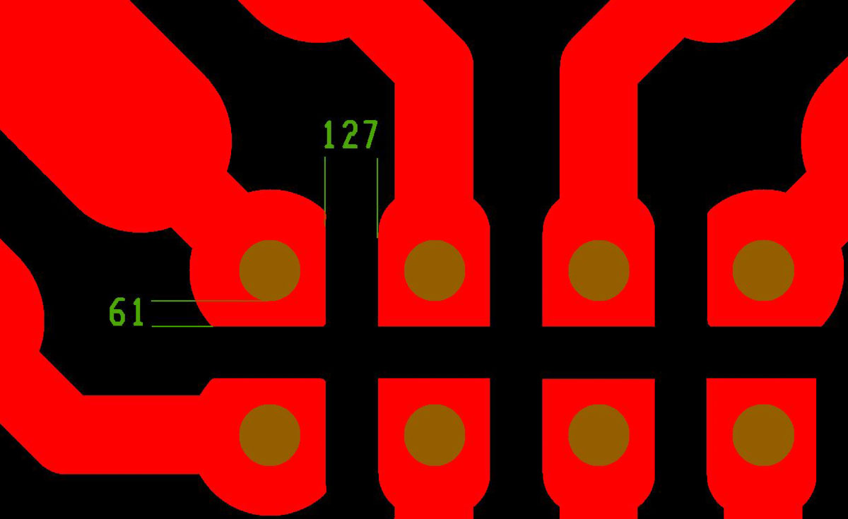
BOT-Side Detail
- Drill: 0.15mm
- Annular ring: varying, min. 61µm
- Via-Pad: varying
- Copper to copper: 127µm
Additional Information:
- Via-in-Pad (see Via Filling)
- Design Parameters
- Basic Design Rules as PDF